Installation
Mounting features
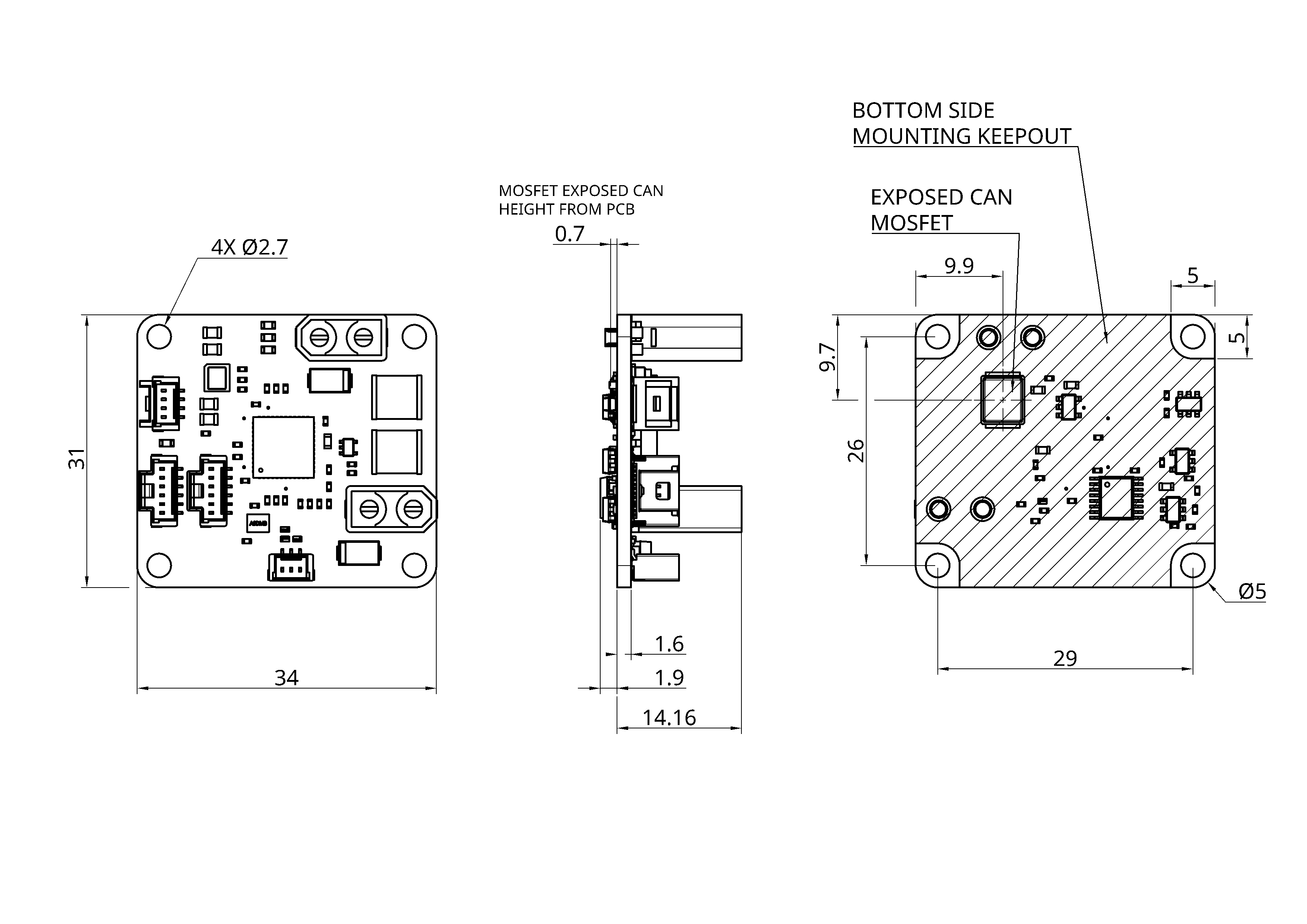
CAD model
Mounting the device
Device has 4x 2.7mm diameter mounting holes, suitable for M2.5 screws. The mounting hole pads are 4.5mm in diameter. Design any mounting posts to be no greater than 4.5mm in diameter.
Consider bottom side components
When mounting the device consider the following:
- The JCS high power voltage supply (up to 72V) can be present on components on the bottom side of the board. Ensure the bottom of the board is electrically isolated from any nearby mounting hardware.
- The package of the bottom power MOSFET is electrically conductive and connected to the source of the MOSFET. Ensure the MOSFET remains electrically isolated at all times.
- Consider the stick-out length of the connectors or soldered power / resistor wires on the bottom of the device.
Thermal Considerations
No heatsink is installed at the factory, ensure the board temperature stays within safe limits.
If further thermal performance is required, the device may be installed onto a suitable plate with a thermally conductive pad sandwiched between the bottom side components and the mounting plate. Exposed package (can) MOSFET location is called out in the mounting drawing. All power components are installed on the bottom side of the device.
Device wiring
Device includes AMASS connectors but these may be replaced with direct wired connection if required.
Consider the following when soldering the wires or connectors into place:
- Ensure no voltage is present on the device or wires!
- Make sure to pre-tin the wires (not necessary for connectors).
- Use flux on the solder pads. The flux residue can be cleaned with an appropriate solvent, eg isopropyl alcohol (IPA).
- Consider the thermal capacity of the PCB. Make sure to use a soldering iron powerful enough to get heat into the wiring and connectors quickly enough as to avoid damage to the device.
- Ensure enough wire is used the the device can be serviced.